In a pioneering achievement, researchers at Tianjin University and the Georgia Institute of Technology have successfully created a fully functional semiconductor using graphene. Walter de Heer and his team expanded upon existing fabrication techniques to introduce a bandgap into the 2D material while preserving graphene's robust and easily tunable properties.
While silicon has long been the cornerstone of modern semiconductor electronics, the latest silicon based technologies are facing challenges in meeting the increasing demands for higher computing speeds, lower power consumption, and more compact devices.
Graphene, first isolated in 2004, has emerged as a promising alternative to silicon. The one atom thick carbon sheet possesses advantageous properties, including high electron mobility, a robust yet lightweight structure, and excellent heat dissipation. The recent breakthrough in creating a functional graphene semiconductor opens new possibilities for advancing electronic devices beyond the limits of traditional silicon based technologies.
One Major Drawback
In contrast to traditional
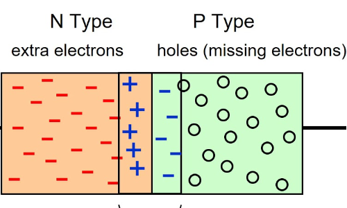
semiconductors, graphene lacks an inherent electron bandgap, an energy barrier crucial for enabling the conduction of electricity. This bandgap is what facilitates the creation of electronic switches, such as transistors, from semiconductor materials.
A persistent challenge in graphene electronics has been the absence of the requisite bandgap, preventing effective switching on and off at the desired ratio. Numerous attempts over the years have been made to address this issue through various methods. Previous studies explored engineering suitable bandgaps using techniques like quantum confinement and chemical modification of pure graphene. Unfortunately, these approaches have seen minimal success.
The process of refining graphene involved extensive learning to enhance its properties and devise methods for accurate property measurement. This intricate process took a considerable amount of time to achieve.
Spontaneous Growth
In their most recent study, researchers have successfully demonstrated the spontaneous growth of the semiconductor "epigraphene" with a bandgap on the surfaces of silicon carbide crystals, marking a groundbreaking achievement.
Prior investigations had indicated that, under high temperatures, silicon undergoes sublimation from the surfaces of these crystals, resulting in the formation of carbon-rich layers. These layers subsequently recrystallize into multi-layered epigraphene, possessing somewhat limited semiconducting properties.
Building upon this method, the team led by de Heer and Ma introduced an innovative annealing technique. By meticulously controlling the sample temperature and the rate of epigraphene formation, they produced a robust graphene layer characterized by macroscopic, atomically-flat terraces. Notably, the alignment of graphene atoms with the lattice of the silicon carbide substrate was achieved through this method.
Useful Bandgap
Through meticulous measurements, the research team established that this layer serves as an exceptional 2D semiconductor. It possesses the elusive and valuable bandgap that researchers have sought for decades, coupled with a high electron mobility.
The newly developed graphene semiconductor is remarkably robust, exhibiting 10 times the electron mobility of silicon. Moreover, it offers unique properties not found in silicon, creating an analogy of comparing electron mobility in silicon to driving on a gravel road, while the epigraphene resembles an electron freeway. This translates to enhanced efficiency, reduced heat generation, and the capability for higher electron speeds.
In addition to its outstanding performance, the team demonstrated the versatility of their epigraphene by doping it with various atoms and molecules to fine tune its electronic and magnetic properties. Furthermore, the material can be nanopatterned to further enhance its performance, a challenging feat with graphene grown on alternative substrates.
This groundbreaking technique holds the potential to revolutionize semiconductor manufacturing, offering a novel approach and marking a crucial initial step towards the development of a new generation of graphene based electronics.
What is a Semiconductor Chip?
A
semiconductor chip material occupies the intermediate space between a conductor and an insulator, exerting control over the flow of electric current in electronic equipment and devices. Consequently, semiconductor devices stand as a widely utilized component in electronic chips designed for computing elements and various electronic devices, including solid state storage.
What is a Semiconductor Optical Amplifier?
A semiconductor optical amplifier (SOA) is a semiconductor component designed to amplify light. SOAs are commonly integrated into optical transceiver modules that facilitate communication between data centers.
The SOA plays a crucial role in amplifying the optical signal utilized for Ethernet communication, effectively compensating for transmission loss.
What is the Difference between an Intrinsic and Extrinsic Semiconductor?
The fundamental distinction between intrinsic and extrinsic semiconductors lies in their composition. Intrinsic semiconductors are pure and consist of a single type of material, devoid of any added impurities.
Conversely, extrinsic semiconductors are impure. They are formed by combining multiple intrinsic semiconductors with additional substances introduced to alter their properties. These added substances commonly involve doping with trivalent or pentavalent impurities.
What is a Fable Semiconductor?
The term "fable," distinct from the semiconductor fabrication (fab), refers to companies engaged in designing, manufacturing, and selling hardware and semiconductor chips without conducting the production of their own silicon wafers or chips. Instead, they opt to outsource the fabrication process to a foundry or another manufacturing facility.
Where Can the Most Semiconductor Chips Be Manufactured?
Despite semiconductors being essential components in the automotive and computing industries for many years, the pursuit of AI dominance and the increasing migration of our digital infrastructure to the cloud have significantly heightened the demand for high-capacity data centers and chip production by companies.
According to data from the semiconductor lobby organization SEMI, approximately 70 percent of the overall manufacturing capacity is concentrated in South Korea, Taiwan, and China. In contrast, the Americas rank fifth, following Japan, which held a 13 percent share in 2022. This distribution marks a significant shift from a few decades ago when, in 1990, the United States accounted for 37 percent of fabrication capacity, Europe contributed another 44 percent, and Japan secured the third position with a 19 percent share. Japan was notably a dominant force in the semiconductor industry in the 1980s, representing 51 percent of global chip sales in 1988. However, the bursting of Japan's economic bubble in the 1990s resulted in the loss of its technological leadership role to Western economies.
Check out all of central semiconductors options to find what you need and contact
GUOYUAN ELECTRONICS for more imformation.