The global demand for reliable, high-performance semiconductor devices, especially in critical areas like automotive, aerospace, and renewable energy (e.g., IGBT modules), necessitates packaging that guarantees long-term protection from environmental ingress. The two greatest enemies of device longevity are moisture/volatiles and oxygen, which contribute to corrosion and bond degradation. Achieving true reliability is a meticulous, multi-stage process, beginning long before the final seal is applied.
While advanced processes like vacuum soldering or welding are often highlighted for the final seal, the preparatory thermal steps—the domain of the hot air oven working principle—are foundational. These steps ensure that the materials are in the optimal state for subsequent high-precision bonding, mitigating latent defects that would otherwise compromise the package integrity. The failure to properly condition materials using uniform heat distribution can render even the most advanced sealing technology ineffective. The foundation of a reliable hermetic package is built on precision thermal preparation.
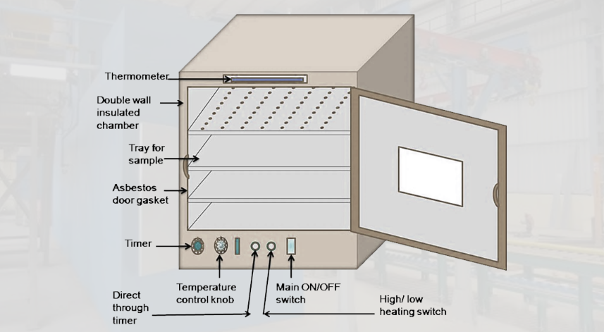
What Is the Primary Function of a Hot Air Oven Working in the Assembly Process?
The hot air oven working in semiconductor manufacturing serves two critical, interconnected functions: curing and drying/outgassing. The efficiency and reliability of both functions depend entirely on the oven’s ability to maintain thermal uniformity and controlled airflow.
Curing of Adhesives and Encapsulants
Many semiconductor devices use polymeric materials—adhesives, epoxies, and underfills—to bond components to substrates or to encapsulate sensitive elements. These materials often require a precise thermal profile to fully polymerize and achieve their specified mechanical and electrical properties.
Temperature Profile Control: The hot air oven working must provide a stable temperature ramp-up, dwell time, and cool-down rate. Deviations in temperature can lead to incomplete curing, leaving soft spots, reduced adhesion strength, or residual chemical activity, all of which compromise reliability.
Stress Management: Non-uniform heat application can create differential thermal expansion across the device and substrate, inducing internal stresses. These stresses, if not properly managed, can lead to cracking, delamination, or wire bond breakage, sometimes years after the device enters service.
Critical Drying and Outgassing (Volatiles Removal)
Perhaps the most essential preparatory role of the hot air oven working principle is the removal of volatile contaminants, chiefly moisture and solvents. Even seemingly dry materials, substrates, and packages absorb trace amounts of moisture from the ambient air.
If these volatiles are not thoroughly removed before the final sealing process, they will outgas when exposed to high processing temperatures or, critically, once the device is sealed. These trapped gases contribute directly to two major failure modes:
Void Formation: Trapped moisture or air expands during subsequent high-temperature processes, forming gas pockets known as voids within the solder joint or adhesive layer.
Package Degradation: Outgassing into the sealed cavity increases the internal pressure and introduces moisture, leading to internal corrosion of the chip or wire bonds, destroying the package’s intended barrier function.
How Does Airflow and Uniformity Define the Hot Air Oven Working Quality?
The difference between a standard industrial oven and a precision hot air oven working in semiconductor assembly lies in its air management system. Achieving true temperature uniformity is a complex thermal engineering challenge.
Forced Convection: The mechanism relies on powerful fans or blowers to circulate heated air throughout the working chamber. This forced convection drastically improves heat transfer efficiency compared to simple radiant or natural convection ovens.
Air Distribution: High-end ovens utilize precise baffling and ducting to ensure the heated air is delivered evenly across the entire product shelf area. This prevents "hot spots" near heating elements and "cold spots" near the walls or exhaust. A variation of even a few degrees Celsius across a large batch can lead to inconsistent curing or incomplete drying for some parts.
Exhaust Management: A controlled exhaust system is vital to properly vent the moisture and solvents released during the outgassing phase, preventing the re-condensation of these contaminants onto other components within the chamber.
Only when the hot air oven working process has completed its task of comprehensive drying and uniform curing can the device transition to the final, highly advanced sealing steps.
Why Must Thermal Preparation Lead to Advanced Vacuum Sealing for True Hermeticity?
Despite the best efforts of the hot air oven working in removing volatiles, the final sealing process presents a new challenge. The highest standard of protection is the hermetic package, defined as a seal that prevents the ingress of external gases over the lifetime of the device, often verified using stringent leak rate standards.
The Void Challenge in Sealing
Many advanced power devices rely on large-area solder or diffusion bonds (e.g., attaching a silicon die to a ceramic substrate). If this bonding occurs in a standard atmospheric environment, two issues arise:
Trapped Air/Nitrogen: During the wetting and flow of the bonding material (solder), small pockets of atmospheric gas can become trapped, leading to voids in the joint.
Oxidation: The high temperatures required for bonding cause rapid oxidation of the bonding surfaces and materials, significantly weakening the final joint integrity and increasing resistance.
The Vacuum Soldering Solution
To solve the void problem completely and achieve a true, long-lasting hermetic seal, an inert or vacuum environment is essential. This is where specialized equipment, such as
Inline Vacuum soldering systems , comes into play.
Void Elimination: By conducting the bonding or sealing process in a high vacuum environment, the opportunity for gas entrapment is virtually eliminated. The vacuum pulls residual gas out of the molten solder before it solidifies, resulting in a joint with near-zero void rate. This is critical for efficient thermal management and mechanical durability in large-area joints.
Perfect Sealing: For metal-to-metal sealing methods, the vacuum process provides an inert atmosphere that prevents oxide formation at the bond interface, ensuring a strong metallurgical bond that guarantees the required hermetic package integrity. This advanced capability is the specialty of dedicated equipment providers like Chengliankaida Technology.co.,LTD, which focuses on high-reliability semiconductor device package production lines.
What is the Relationship Between Void Rate and a Device’s Long-Term Reliability?
The ability to maintain a low void rate—made possible by effective pre-treatment from the hot air oven working process followed by precise vacuum sealing—is not merely an aesthetic requirement; it is a fundamental reliability factor.
Thermal Management: In power devices (like IGBTs or MOSFETs), heat dissipation is paramount. Voids within a solder joint act as thermal insulators, creating localized hot spots. These hot spots accelerate device degradation, decrease efficiency, and ultimately lead to premature failure due to thermal cycling fatigue. Reducing voids ensures efficient and uniform heat transfer away from the sensitive chip.
Mechanical Strength: Voids reduce the effective cross-sectional area of the bond, making the joint structurally weaker. This weakness makes the device more susceptible to failure caused by external shock, vibration, or the internal stresses generated by temperature fluctuations during operation.
How Are Industry Standards Driven by Advanced Manufacturing Responsibility?
As devices become smaller, more powerful, and operate in harsher conditions, the standards for quality control must continually rise. The success of a hermetic package is often measured by its compliance with military or industrial standards (e.g., MIL-STD-883) for leak testing. Achieving these standards consistently requires manufacturers to operate with a high degree of technical responsibility.
Companies that prioritize "Honesty & Innovation & Intelligent & Manufacturing Responsibility" invest heavily in research and development to push the boundaries of achievable manufacturing precision. This commitment extends from optimizing the basic hot air oven working parameters to developing cutting-edge vacuum systems, leading to a demonstrable reduction in manufacturing defects and an improvement in device life. The future of high-reliability semiconductor technology rests on the continuous improvement of every step, from initial thermal preparation to final vacuum sealing, supported by innovators like Chengliankaida Technology.
Comments