Semiconductor manufacturing is a complex process involving multiple stages, with the front-end and back-end processes being the two primary divisions. While both are critical to the production of functional semiconductor devices, they differ significantly in terms of their objectives, processes, and tools used. As a high-tech company specializing in the development of vacuum welding machines and production lines for semiconductor device packaging, Chengliankaida Technology understands the significance of the back-end semiconductor manufacturing process. This article will delve into the key differences between front-end and back-end manufacturing and how these stages contribute to the final semiconductor device.
Front-End Semiconductor Manufacturing Process
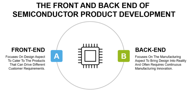
The front-end semiconductor manufacturing process is the initial stage in the semiconductor fabrication process. It involves the creation of semiconductor wafers from raw materials and the preparation of these wafers for future device fabrication. The key activities in the front-end process are:
1. Wafer Fabrication
The front-end process begins with the production of a semiconductor wafer, typically made from silicon, although other materials like gallium arsenide are also used. This wafer undergoes various steps such as:
- Oxidation: The wafer is exposed to oxygen at high temperatures to create a thin oxide layer, which serves as an insulator.
- Photolithography: Using light-sensitive chemicals, intricate patterns are etched onto the wafer to define the circuits and features of the semiconductor devices.
- Deposition and Etching: Layers of metal and insulating materials are added and selectively etched to form the desired structures on the wafer.
2. Doping
Doping is the process of introducing impurities into the silicon wafer to modify its electrical properties. Different areas of the wafer are doped with various materials like phosphorus or boron, creating regions of different electrical conductivities.
3. Circuit Formation
After doping, photolithography and etching are used again to create the specific circuit patterns. This involves precise control to ensure that each device on the wafer meets the required performance specifications.
4. Testing
The front-end process includes several testing phases, primarily focused on assessing the electrical characteristics of the semiconductor devices at the wafer level. This is done before the wafer undergoes any further processing.
The front-end process ends once the wafer has been fully processed, and the individual chips are ready to be cut out for further assembly.
Back-End Semiconductor Manufacturing Process
The back-end semiconductor manufacturing process focuses on the assembly, packaging, and testing of individual semiconductor chips. This stage is essential in ensuring that the fabricated semiconductor devices meet performance, durability, and reliability standards. The back-end process includes several key steps:
1. Wafer Dicing
After the front-end process, the wafer is divided into individual semiconductor chips through a process called wafer dicing. The wafer is cut into smaller units, each of which will eventually become a finished chip.
2. Die Bonding
Die bonding refers to the process of attaching the individual chips (or dies) to a substrate. This is usually done using specialized materials like conductive epoxy or solders. The choice of bonding material depends on the performance requirements and the application of the semiconductor device.
3. Wire Bonding
Once the dies are bonded to the substrate, fine wires are used to establish electrical connections between the chip and the package. This step ensures that the chip can interface with the outside world and perform its intended function.
4. Packaging
Packaging is one of the most crucial stages in the back-end semiconductor manufacturing process. The chip is enclosed in a protective shell, which can be made from materials such as plastic, ceramic, or metal. The package provides mechanical support, electrical connections, and protection from environmental factors like moisture and heat.
Chengliankaida Technology’s Role: As a high-tech enterprise specializing in vacuum welding machines, Chengliankaida contributes to the back-end process by providing advanced equipment used in the packaging of power devices and semiconductor electronic devices. Our vacuum welding machines are essential for achieving high-quality hermetic seals, which are critical in ensuring the reliability and performance of semiconductor devices, especially in high-power applications such as IGBT (Insulated Gate Bipolar Transistor) modules.
5. Testing and Quality Control
The final stage in the back-end process is testing. This involves rigorous testing procedures to ensure that the chip meets all performance specifications and can function reliably under real-world conditions. Some common tests include:
- Functional Testing: Verifying the chip's electrical performance.
- Burn-In Testing: Subjecting the device to high stress to detect potential failures.
- Reliability Testing: Assessing the device’s long-term performance.
- Once the testing is complete, the packaged semiconductor chips are ready for shipment to customers.
Key Differences Between Front-End and Back-End Processes
While both the front-end and back-end semiconductor manufacturing processes are necessary for producing functional semiconductor devices, they differ significantly in terms of their focus, techniques, and tools:
1. Focus
- Front-End: Primarily focused on wafer fabrication, circuit formation, and doping.
- Back-End: Focused on assembly, packaging, and testing of individual semiconductor devices.
2. Equipment Used
- Front-End: Requires photolithography equipment, ion implanters for doping, and deposition systems.
- Back-End: Requires packaging equipment, die bonders, wire bonders, and vacuum welding machines for hermetic sealing.
3. Skill Set and Expertise
- Front-End: Involves expertise in materials science, microelectronics, and photonics.
- Back-End: Requires knowledge in packaging, mechanical engineering, and reliability testing.
4. Outcomes
- Front-End: Results in processed wafers with individual semiconductor devices still attached.
- Back-End: Results in fully packaged semiconductor devices ready for use in electronic products.
Conclusion
In conclusion, both front-end and back-end semiconductor manufacturing processes are vital to producing reliable and high-performance semiconductor devices. While the front-end process is focused on wafer fabrication and circuit formation, the back-end process is centered on packaging, testing, and ensuring that the final product is functional and durable.
Chengliankaida Technology, with its expertise in vacuum welding machines, plays a crucial role in the back-end process, particularly in providing high-quality hermetic sealing solutions for power devices and semiconductor electronic devices.
As the semiconductor industry continues to evolve, the front-end and back-end processes will remain crucial in shaping the next generation of semiconductor technologies. At Chengliankaida, we remain committed to innovation and advancing semiconductor device packaging through our cutting-edge technology and expertise.
Comments